晶振官方博客
更多>>晶振資料
來源:http://m.dxwyp.cn 作者:konuaer 2012年04月23
Kang Waldorf Electronics Co., Ltd. - quartz crystal design circuit Guide
Sport Waldorf electronics: the night of the continuous development of growth, from civil crystal, industrial crystal, military crystal, from the DIP crystal oscillator, SMD crystal, ceramic atomization piece, satellite navigation, SAW filter series.
From chip research and development, circuit design. The company already has the technology and development of production capacity, now some crystal design circuit, 32.768K kHz crystal matching capacitor, crystal match the IC, the crystal oscillation mode, the drive voltage and power, the welding temperature curve application published, I hope this can help to the needy and design to
Oscillation Circuit Design Overview
Oscillation Circuit Design Key Parameters
DRIVE LEVEL (DL), OSCILLATION FREQUENCY AND LOAD CAPACITANCE (CL),
OSCILLATION ALLOWANCE, FREQUENCY-TEMPERATURE CURVE
DRIVE LEVEL (DL)
The drive level of a crystal unit is shown by the level of the operating power or the current consumption (see Figures 9,10, and 11). Operating the crystal unit at an excessive power level will result in the degradation of its characteristics, which may cause frequency instability or physical failure of the crystal chip. Design your circuit within absolute maximum drive level.
.jpg)
OSCILLATION FREQUENCY AND LOAD CAPACITANCE (CL)
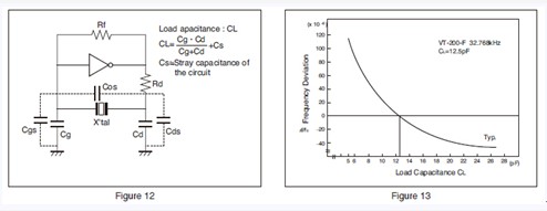
The load capacitance (CL) is a parameter for determining the frequency of the oscillation circuit. The CL is represented by an effective equivalent capacitance that is loaded from the oscillation circuit to both ends of the crystal unit (see Figure 12). The oscillation frequency varies depending upon the load capacitance of the oscillation circuit. In order to obtain the desirable frequency accuracy, matching between the load capacitances of the oscillation circuit and the crystal unit is required. For the use of the crystal unit, match the load capacitances of the oscillation circuit with the load capacitances of the crystal unit.
 OSCILLATION ALLOWANCE
To ensure stable oscillation, the negative resistance of the circuit should be significantly larger than the equivalent series resistance (the oscillation allowance is large). Ensure that the oscillation allowance is at least five times as large as the equivalent series resistance.
Oscillation Allowance Evaluation Method
Add resistor "Rx" to the crystal unit in series and ensure that the oscillation starts or stops. The approximate negative resistance of the circuit is the value obtained by adding the effective resistance "Re" to the maximum resistance "Rx" when the oscillation starts or stops after gradually making Rx value larger.
Negative resistance |- R| = Rx + Re
|−R| is a value at least five times as large as the maximum equivalent series resistance (R1 max.) of the crystal unit.
*Re is the effective resistance value during oscillation.
Re = R1 (1 + CO/CL ) 2
.JPG)
FREQUENCY-TEMPERATURE CURVE
.jpg)
Frequency temperature characteristics of tuning fork crystals is shown by negative quadratic curve which has a peak at 25ºC as per left graph.
Please make sure to consider the temperature range and frequency accuracy you need since magnitude of frequency variation becomes larger and larger as the temperature range becomes wider.
[Approximation formula of frequency temperature characteristics]
f_tem = B(T-Ti) 2
B : Parabolic coefficient
T : Given temperature
Ti : Turnover temperature
Sport Waldorf electronics: the night of the continuous development of growth, from civil crystal, industrial crystal, military crystal, from the DIP crystal oscillator, SMD crystal, ceramic atomization piece, satellite navigation, SAW filter series.
From chip research and development, circuit design. The company already has the technology and development of production capacity, now some crystal design circuit, 32.768K kHz crystal matching capacitor, crystal match the IC, the crystal oscillation mode, the drive voltage and power, the welding temperature curve application published, I hope this can help to the needy and design to
Oscillation Circuit Design Overview
Oscillation Circuit Design Key Parameters
DRIVE LEVEL (DL), OSCILLATION FREQUENCY AND LOAD CAPACITANCE (CL),
OSCILLATION ALLOWANCE, FREQUENCY-TEMPERATURE CURVE
DRIVE LEVEL (DL)
The drive level of a crystal unit is shown by the level of the operating power or the current consumption (see Figures 9,10, and 11). Operating the crystal unit at an excessive power level will result in the degradation of its characteristics, which may cause frequency instability or physical failure of the crystal chip. Design your circuit within absolute maximum drive level.
.jpg)
OSCILLATION FREQUENCY AND LOAD CAPACITANCE (CL)
The load capacitance (CL) is a parameter for determining the frequency of the oscillation circuit. The CL is represented by an effective equivalent capacitance that is loaded from the oscillation circuit to both ends of the crystal unit (see Figure 12). The oscillation frequency varies depending upon the load capacitance of the oscillation circuit. In order to obtain the desirable frequency accuracy, matching between the load capacitances of the oscillation circuit and the crystal unit is required. For the use of the crystal unit, match the load capacitances of the oscillation circuit with the load capacitances of the crystal unit.
 OSCILLATION ALLOWANCE
To ensure stable oscillation, the negative resistance of the circuit should be significantly larger than the equivalent series resistance (the oscillation allowance is large). Ensure that the oscillation allowance is at least five times as large as the equivalent series resistance.
Oscillation Allowance Evaluation Method
Add resistor "Rx" to the crystal unit in series and ensure that the oscillation starts or stops. The approximate negative resistance of the circuit is the value obtained by adding the effective resistance "Re" to the maximum resistance "Rx" when the oscillation starts or stops after gradually making Rx value larger.
Negative resistance |- R| = Rx + Re
|−R| is a value at least five times as large as the maximum equivalent series resistance (R1 max.) of the crystal unit.
*Re is the effective resistance value during oscillation.
Re = R1 (1 + CO/CL ) 2
.JPG)
FREQUENCY-TEMPERATURE CURVE
.jpg)
Frequency temperature characteristics of tuning fork crystals is shown by negative quadratic curve which has a peak at 25ºC as per left graph.
Please make sure to consider the temperature range and frequency accuracy you need since magnitude of frequency variation becomes larger and larger as the temperature range becomes wider.
[Approximation formula of frequency temperature characteristics]
f_tem = B(T-Ti) 2
B : Parabolic coefficient
T : Given temperature
Ti : Turnover temperature
正在載入評(píng)論數(shù)據(jù)...
此文關(guān)鍵字: 晶振資料石英晶體線路設(shè)計(jì)資料
相關(guān)資訊
- [2022-09-07]出色穩(wěn)定性能的5032mm石英晶體振蕩器X1...
- [2022-08-01]diodes晶振專用于時(shí)間顯示設(shè)備的32.768...
- [2022-07-27]伊西斯的新型且創(chuàng)意的低姿態(tài)TCXO晶體振...
- [2020-06-22]深入探討有源晶振8個(gè)基礎(chǔ)參數(shù)詞匯
- [2020-05-25]SiTime開發(fā)的新軟件可模擬振蕩器時(shí)間誤...
- [2020-05-12]微處理器應(yīng)該怎樣選擇匹配晶振?一文足...
- [2020-04-14]NDK株式會(huì)社差分振蕩器NP3225SBB規(guī)格更...
- [2020-03-13]不同類型的Crystal Oscillator工作與電...
- [2019-11-09]了解EPSON晶振獨(dú)特的封裝技術(shù)
- [2019-09-21]NDK振蕩器電路圖介紹及安裝示例
- [2019-09-16]擁有聲子晶體結(jié)構(gòu)的AT切割諧振器共振分...
- [2019-09-04]SMD Oscillator高溫回流焊接的滯后反應(yīng)...


 銷售代表
銷售代表 售后服務(wù)
.jpg)
.jpg)